Bottom image: A chip that can help instruments on distant planets hunt for signs of life. This chip has a self contained analysis environment.
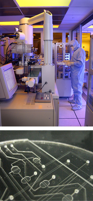
JPL’s Microdevices Laboratory, or MDL, is a first-rate space microelectronics fabrication facility containing over 130 individual pieces of processing equipment, including systems for UV contact and projection lithography, electron-beam lithography, materials growth and deposition, wet and dry etching, thermal processing and optical, structural and electronic characterization.
The heart of the MDL is a 13,000-square-foot clean room that is used by over 70 research scientists. The clean room is divided into various zones according to cleanliness standards, ranging from class 100,000 for the rooms housing epitaxial deposition systems, to class 10 for the lithography area.
Developing a unique JPL capability
Microdevice fabrication requires sophisticated equipment for the deposition, etching and patterning of device layers, and must generally be done in a very clean environment to avoid contamination and defects. As a result, it has been highly desirable for JPL to centrally locate such activities, to allow expensive equipment to be shared and to spread the maintenance burden over a larger base of activity. In 2008, the facility celebrated 20 successful years of developing technologies and devices to enable and enhance space missions.
While industrial fabrication labs are usually designed for mass production of devices using a standard process, the MDL is much more flexible, allowing research, development and small-scale production of a broad range of devices. The MDL functions as a multi-user and shared-equipment facility that is open to all JPL personnel. MDL access for users from outside institutions can also be arranged.
Continuous investment in MDL’s processing equipment is essential. The equipment for micro- and nano-fabrication continues to develop at a very rapid pace, driven primarily by the semiconductor industry, and the timescale for obsolescence is short. As a result, in some cases MDL is able to acquire previous-generation production equipment at a substantial discount; a good example is MDL’s primary photolithography tool, the Canon EX3 deep-UV projection lithography system, which is capable of 0.25-micrometer resolution. However, because the MDL focuses on unique devices for space applications rather than the mass production of commodity chips, production equipment is not always suitable— MDL equipment is often smaller in scale, and may be custom built for specific requirements. The dedicated ultra-high vacuum (UHV) sputtering systems used to deposit superconducting films are examples of the latter category.
Some MDL highlights
- MDL’s world-class electron beam lithography system uses a focused beam of electrons to write patterns directly onto wafers. This powerful capability allows MDL technologists to create atomic-scale features as small as 4 nanometers (see image at right-top).
- The European Space Agency’s recently launched Herschel and Planck missions rely on a number of MDL produced technologies, including spider web bolometers, which are currently the most sensitive direct detectors for light in the far-infrared range.
- The MDL recently installed a new silicon Molecular Beam Epitaxy, or MBE, machine which has the capacity to process up to eight-inch silicon wafers. MBE allows the growth of crystalline samples with extremely precise control, so that structures can be built up a single atomic layer at a time. The MBE technique is applicable to a wide variety of compound semiconductors. With JPL’s investment in this new capability, it will be possible to respond to the demands of producing a large number of large-format detector arrays for next-generation space missions.
- MDL has partnered with the University of California at Berkeley and NASA’s Ames Research Center to develop “lab on a chip” systems to investigate the presence of organic compounds in the Martian regolith, as well as sensors to assess the oxidation effects that the Mars environment would have on possible organic material (see image at right-bottom).
Visit the JPL Microdevices Laboratory website for additional information.