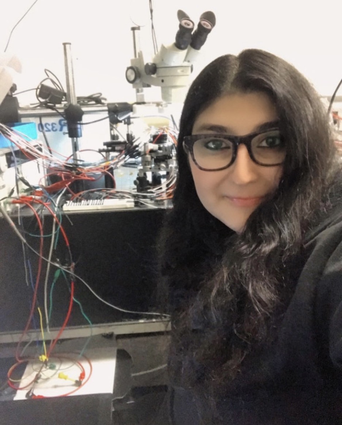
Dr. Hani Nejadriahi is a postdoctoral fellow at JPL’s Microdevices Laboratory, where she does research and development of integrated-photonic technologies for space applications.
Hani’s work focuses on design, modeling, fabrication, and characterization of passive and active photonic integrated circuits (PICs) in novel materials such as ultra-low loss silicon nitride and gallium nitride that she develops in-house.
Silicon nitride (Si3N4) due to its broad transparency window which extends from UV to NIR (200 to ~2500 nm), low losses (~ <10 dB/m), high optical power handling (due to negligible TPA), thermal stability, customizability and integration capabilities plays a crucial role in the development of laser optics systems for cold atom sensors and applications.
In particular as part of current efforts at MDL towards the laser optics improvements and miniaturization of cold atom sensors, after realizing a ~ 1dB/m loss Si3N4 platform at 780-852 nm, Hani has focused on development of ultra-narrow linewidth external cavity lasers around these wavelengths since commercial lasers are either not available at these wavelengths or are not narrow-linewidth enough. Hence bringing this technology to MDL/JPL is of utmost importance for many applications that benefit from having integrated narrow linewidth lasers.
Additionally, to build a fully working system on-chip, more devices are currently under development by her such as wavemeter, phase modulator/switches, isolators, and passive components such as splitters, couplers and interferometers.
On the other hand, Gallium nitride is a well-established compound semiconductor with many advantages in different functionalities and application due to its piezoelectricity, transparency around UV and visible wavelengths (good coverage around 780-852nm), and the ability to confine acousto-optical interaction with efficient device designs via lithographic control at wavelength scales. Hani actively is working under the Advanced Component Technology (ACT) program where she designs, fabricates, and characterizes acousto-optic devices in GaN-on-Sapphire to achieve high performance acousto-optic modulator (AOM) with mW-level drive powers.
These waveguide platforms enable low SWaP and reliable next generation of devices and systems of interest to many NASA applications spanning from Earth Sciences (i.e., cold atom sensors) to astrophotonics (for coronographs, wavefront correction, and spectrographs). These PICs are wavelength agnostics and can operate at any wavelength depending on the bandgap of the material they are designed in and are a fertile ground to explore new type flight compatible systems.
In addition to her integrated photonics work, Hani works on design and fabrication of diffractive optical elements using both binary and greyscale lithography (i.e., gratings for spectrometers, lenses, etc). Many of these components are essential part of many flight projects at JPL.
- PhD, Electrical Engineering, Photonics, University of California, San Diego (2022)
- MSc, Electrical Engineering, Photonics, George Washington University, (2017)
- BA, Mathematics, Physics, Music Performance, St. Olaf College (2014)
Integrated Photonics for low SWaP component and system developments in Astrophotonics (nulling interferometer, wave-front sensing, integrated coronagraphs) and Earth Science applications (Quantum Gravity Gradiometer)
- Mid-long infrared device development and technologies
- Nonlinear Optics
- Quantum Sensors and laser cooling applications
- Remote Sensing/LiDAR
- Optical Communications
- Postdoctoral Scholar, Jet Propulsion Laboratory, California Institute of Technology (2022 - Present)
- IEEE Women in Photonics Chair (2022- Present)
- Optical Engineer (AR/VR)- Part time, Amazon Lab 126 (Jan 2022-May 2022)
- Graduate Student Researcher, University of California, San Diego (2017-2022)
- Graduate Researcher- Internship, Jet Propulsion Laboratory, California Institute of Technology (2021)
- Graduate Student Researcher, George Washington University, Washington DC (2015-2017)
- Process Engineer, SAGE Electrochromics- Saint Gobain, (2014-2015)
- PhD Fellowship, University of California, San Diego (2017-2022)
- MSc Fellowship, George Washington University (2015-2017)
- Best Presentation among three REU programs, University of Maryland, College Park (Summer 2013)
- Music Scholarship, St. Olaf College, (2010-2014)
- Buntrock’s (Science and Math) Scholarship, St. Olaf College, (2010-2014)
- National Merit Scholarship (Illinois), (2010)
- H. Nejadriahi, E. Kittlaus, S. Forouhar, “Low loss silicon nitride for application in cold atom sensors”, SPIE Optics + Photonics (August 2023)
- H. Nejadriahi, A. Friedman, R. Sharma, S. Pappert, Y. Fainman, and P. Yu, "Thermo-optic properties of silicon-rich silicon nitride for on-chip applications," Opt. Express 28, 24951-24960 (2020)
- H. Nejadriahi, S. Pappert, Y. Fainman, and P. Yu, "Efficient and compact thermo-optic phase shifter in silicon-rich silicon nitride," Opt. Lett. 46, 4646-4649 (2021)
- H. Nejadriahi, P. Gaur, K. Johnson, S. Pappert, Y. Fainman, and P. Yu, "Realization of a wide steering end-fire facet optical phased array using silicon rich silicon nitride," Opt. Lett. 48, 807-810 (2023)
- A. Friedman, H. Nejadriahi, R. Sharma, and Y. Fainman, "Demonstration of the DC-Kerr effect in silicon-rich nitride," Opt. Lett. 46, 4236-4239 (2021)
- L.Y. S. Chang, H. Nejadriahi, S. Pappert, and P. K. L. Yu, “Demonstration of DC Kerr effect induced high nonlinear susceptibility in silicon rich amorphous silicon carbide", Appl. Phys. Lett. 120, 071107 (2022).
- H. Nejadriahi, A. Friedman, R. Sharma, S. Pappert, Y. Fainman and P. Yu, "Enhanced thermo-optic effect in PECVD deposited silicon-rich silicon nitride," 2020 IEEE Photonics Conference (IPC), Vancouver, BC, Canada, 2020, pp. 1-2, doi: 10.1109/IPC47351.2020.9252294.
- H. Nejadriahi, S. Pappert, Y. Fainman and P. Yu, " Silicon rich silicon nitride for efficient thermooptic switches," 2021 Advanced Photonics Congress (APC), Montréal, Quebec, Canada, 2021, pp. 1-2, Control ID: 3579314
- H. Nejadriahi, D. HillerKuss, J. K. George, V. J. Sorger, "Integrated All-Optical Fast Fourier Transform: Design and Sensitivity Analysis", arXiv:1711.02500. (2017)
- H. Nejadriahi and V. J. Sorger, "On-chip Integrated All-Optical Fast Fourier Transform: Design and Analysis," in Frontiers in Optics 2017, OSA Technical Digest (online) (Optical Society of America, 2017), paper JW4A.46.
- J. George, H. Nejadriahi, V. Sorger, "Towards On-Chip Optical FFTs for Convolutional Neural Networks", IEEE International Conference on Rebooting Computing. (2017)
- H. Nejadriahi, V. Sorger, US Patent Granted US20190072833A1: “All optical fast Fourier transform on chip with heating tunability design, simulation, fabrication, and performance analysis”