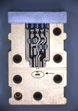
JPL’s Submillimeter Wave Advanced Technology, or SWAT, lab has produced the first example of an amplifier module for submillimeter waves combined into a single-chip with its waveguide connections. The integrated module creates a high-performance, low-loss means of packaging this type of chip in a waveguide for use at frequencies above 300 GHz. The JPL team, led by Lorene Samoska, has developed the amplifier module for a DARPA SWIFT Program as part of a submillimeter-wave imager.
Submillimeter-wave technology has exciting applications to radio astronomy. The European Space Agency’s Herschel and Planck spacecraft, slated for a dual launch this spring, will both image the sky at submillimeter frequencies. JPL provided key technology for two instruments onboard the Herschel spacecraft.
In general, submillimeter-wave imaging is a growing field, with a variety of potential security-related applications, including detection of hidden explosives and bioweapons. A submillimeter-wave amplifier could provide better signal-to-noise for such an imaging system, allowing detection of a concealed metal object under clothing or enabling a helicopter pilot to see through a dust storm.
Longer wavelength microwaves can be transmitted via coaxial cable, but the cables are lossy at higher frequencies. Thus, submillimeter waves require a waveguide solution for transmitting an RF signal. The major challenge is that, as the signal propagates from a material with a lower dielectric constant, or permittivity, into one with a higher dielectric constant, some of the signal's power will be lost. Thus the principle criterion for the JPL team was to efficiently couple the signal from the low-permittivity waveguide channel to the high permittivity MMIC microstrip with as little degradation of the signal as possible.
This type of amplifier component – a monolithic millimeter wave integrated circuit, or MMIC – is well established for lower frequencies, and typically uses wire bonds to bridge the transition between a waveguide channel probe and the semiconductor chip. But the bonds themselves cause bandwidth and signal loss problems at frequencies above 200 GHz. The JPL chip gets rid of the wire bonds and pushes the highest reported operating frequency for an amplifier module from the previous limit of 230 GHz to 345 GHz. Additionally, the design of a single, integrated module without wire bonds also allows the unit to be dropped into a waveguide module for ease of fabrication.
The packaged amplifier chip combines submillimeter-wave design techniques traditionally used for passive components with lower frequency, transistor-based MMIC packaging techniques. Samoska says the module opens the door for implementation of submillimeter-wave amplifiers at higher frequencies and for greater sensitivity in imaging systems and heterodyne receivers.
The work was a collaboration between JPL and Northrop Grumman Corporation (NGC), which developed the thin-film MMIC design and manufacturing process employed to produce the MMIC chip.
Contributors include Goutam Chattopadhyay, David Pukala, Andy Fung, Todd Gaier and Mary Soria of JPL, and William Deal, Vesna Radisic, Xiaobing Mei and Richard Lai of NGC, with support from Dr. Mark Rosker of DARPA and Dr. Alfred Hung of Army Research Laboratory.
Contact Informaiton
Lorene Samoska - Technical Contact
E-Mail - Lorene.Samoska@jpl.nasa.gov
Phone - 818.354.0849